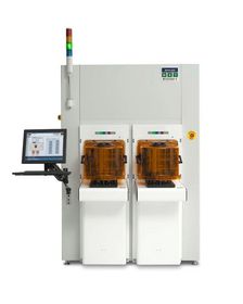
SAN JOSE, CA--(Marketwired - Jul 13, 2015) - Marking an important milestone for its Molecular Vapor Deposition (MVD®) technology, Applied Microstructures (AMST) today announced that it will ship its 100th tool to a semiconductor manufacturer in Asia next week. AMST technology and equipment is used to volume-produce MEMS devices found in smartphones, computers, automobiles, and products that enable the Internet of Things (IoT). The customer selected MVD for its proven capability to improve yield and device performance, and for the tool's very high reliability. They're the latest to deploy AMST's MVD platform which is used by customers worldwide to build MEMS devices like gyroscopes, digital displays, motion sensors, microphones, and accelerometers.
Since its debut in 2004, more than 7 billion MEMS devices have been produced with the help of MVD technology.
"This milestone order highlights the growing adoption of our MVD technology," said AMST Chief Executive Officer Ken Aitchison. "With systems installed in every semiconductor manufacturing region, our technology is valued as an important enabler of devices that power the products at the center of our connected lives."
MVD: A One-of-a-Kind Technology for Anti-Stiction Coatings
MVD was invented by AMST to help semiconductor manufacturers grow ultra-thin, functionalized, organic and inorganic films with higher yields and better cost efficiencies than traditional liquid deposition techniques. Such films serve as lubricant, protective, hydrophobic, hydrophilic, biocompatible, or reactive coatings. In MEMS applications, for example, MVD films are typically used as anti-stiction coatings to improve device performance, and enhance overall device lifetime.
MVD process technology deposits ultra-thin films by vapor deposition at low temperatures on a broad spectrum of substrates. It's the only deposition technology of its kind. A highly flexible system that can run both ALD-like and CVD-like processes, the platform features an integrated microwave plasma for substrate conditioning. MVD platforms allow for the use of up to four precursors, and can process up to 25 300mm wafers or other three-dimensional objects in a single batch. It delivers extremely high conformality on aggressive aspect ratios of up to 2000:1.
With MVD, manufacturers can achieve exceptional film uniformity with industry-leading reliability -- advantages that maximize manufacturing yields and reduce overall costs. Device performance is also greatly improved, especially in many MEMS applications. For example, with MVD-deposited anti-stiction films, failure rates for microphones shrank from 14 percent to 0.4 percent, while the failure rate for accelerometers dropped from 40 percent to less than 5 percent.
The MVD platform is versatile, easy-to-use and highly scalable. In addition, the learning curve is light, which is a benefit valued by customers who deploy the system for multiple applications. The ultra-low cost-of-ownership is due to the tool's inherent efficiencies, and further enabled by its very low precursor consumption. Also, by consuming only milligram levels of precursor per run, and requiring nearly zero point-of-use exhaust treatment, it's greener than most other CVD deposition techniques.
Calling MVD a superior alternative to traditional methods for growing ultra-thin protective films, Aitchison added, "With feature sizes shrinking faster than the pace of progress for conventional deposition tools, MVD presented a completely new approach. Unburdened by legacy technologies, the platform was engineered by our team of thin-film deposition experts and built specifically to meet the aggressive performance specs for today's advanced devices. Our 100-tool milestone was reached thanks to close collaboration with customers and our tradition of providing application-specific technology solutions. We're excited to continue our growth and extend our technology's value to yet more customers."
Beyond MEMS, other important applications benefit from MVD. In advanced packaging applications for example, MVD films are used as moisture barriers for polymers, as well as oxidation and corrosion barriers on metals. In inkjet applications, MVD films can prevent ink accumulation on the nozzle face plate to optimize ink flow. In bio-MEMS, MVD films improve wetting and/or prevent protein adsorption. In biotechnology applications, MVD films are used to create surface anchors for biomolecule reactions. In nano-imprint lithography, MVD films are used as very thin and conformal release layers between the stamp and polymer materials.
AMST's family of MVD products include the MVD100E, MVD300 and MVD4500.
For more information about MVD technology, as well as MVD applications and AMST services, please visit us at www.appliedmst.com.
About Applied Microstructures
Applied Microstructures, Inc. (AMST) helps leading manufacturers make microelectronics found in mobile devices, as well as computing, automotive and other applications that enable the Internet of Things. The company pioneered Molecular Vapor Deposition (MVD®), a unique technology used to deposit anti-stiction and other ultra-thin films used to build MEMS devices, like digital displays, motion sensors, microphones, and accelerometers. Customers rely on MVD to achieve exceptional film uniformity with very high reliability -- advantages that increase yield, boost device performance, and lower overall costs. Founded in 2003, venture-backed AMST is headquartered in San Jose, Calif., with sales and support operations located globally. www.appliedmst.com
MVD is trademarked by Applied Microstructures, Inc.
Contact Information:
Contact:
Jane Evans-Ryan
Genuity PR for AMST
m +1 408 489-6391
email:
